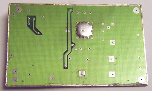
Photo shows the reverse of the PCB with the raised blob of solder where the green solder resist has been scraped off both sides of the PCB to enable the AD9852 to be soldered to the PCB using a 40W soldering iron
- Note that the corner vias are not involved in this.
It is necessary the scrape the resist off the back as well as the front of the PCB to enable the soldering iron to conduct to all vias simultaneously. The raised blob of solder enables sufficient pressure head to overcome the capilliary attraction of the solder staying in the via, but without forcing surplus solder out to bridge the connecting pads.
It seems to work OK - but remember to flux the parts before assembly - it makes a big difference to solder flow.
 E-Mail: davidwrigley@microwave.fsnet.co.uk
Last updated 2004 Jul 12